
loading...
Low power design is a necessity today in all integrated circuits. In this article, I plan to cover the basic techniques of low power design independent of tools.
As companies, started packing more and more features and applications on the battery-operated devices (mobile/ handheld/ laptops), battery backup time became very important. Power consumption slowly became an increasingly important criterion from the customers. Due to this, all chip companies (having products for battery-operated devices) are focusing on lower power consumption. There are efforts to reduce dynamic as well as static power consumption. Companies started to reduce the nominal voltages inside the chip, however, this was also limited along with the technology. So a lot of low power design techniques started to get employed during the Chip Design process to reduce both static and dynamic power consumption. Here’s a list of the popular and commonly used Low Power Design Techniques:
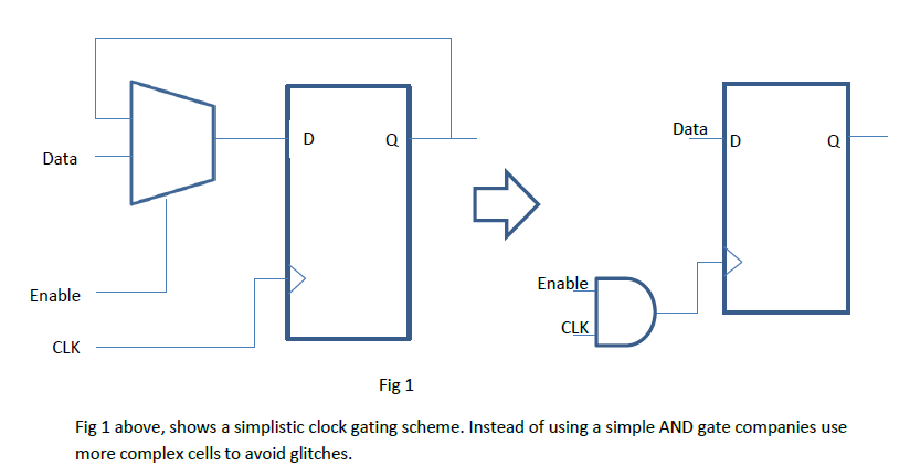
This was by far one of the first techniques to save power (and it also results in saving some area due to sharing, however, it makes the design slightly difficult for timing and DFT). The thought here is that if a common clock signal is going to hundreds of flops, a lot of them are retaining their old value, then we can gate off the clock to such flip flops and they still retain their old value. This gating off results in lesser toggling in the clock path cells and thus saves dynamic power. Nowadays, synthesis tools identify chunks of flip flops that have a common structure and common enable of loading data and covert all such structures into clock gating cells.
In a practical device/ application, a large portion of the ICs is not in use for a reasonable amount of time. If the power to such a portion of the IC can be switched off, it can save a lot of power. This saves static (leakage) power and can save some dynamic power as well where the clock was not gated off. Following are considerations that have to be taken for such a technique:
a. Complexity for Application Development: One of the penalties here is that portion being switch off shall need to be re-configured by software after power is switched on for that portion of the chip. In large cases, this penalty is negligible and so this is also one of the simplistic and commonly used techniques nowadays.
b. Complexities in power Backend Flow: Power Grid Design, Synthesis, Placement, Clock Tree, Static Timing Analysis c. Complexity in logic design: Isolation cells, Power Off scheme and Power on the scheme for the logic going off.
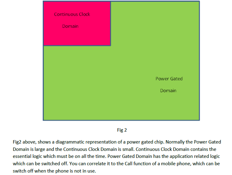
We need to control the signal values, which are output from the gated off portion. As power is gated off, outputs from the Power Gated Domain shall start to float to un-known values. However, there may be cells, in the Continuous Clock Domain, sampling the signals from Power Gated Domain. Such cells will give incorrect output if they sample un-known or floating values. Also, normally a static value (reset value or off state value) is sufficient to continue the normal functioning of the Continuous Clock Domain cells. So we need to isolate such floating values and give logic 0 or logic 1 to signals from the Power Gated Domain. So a different type of cell was designed for this – Isolation cells. For the Power on/ off the flow, a low power controller can be created in the Continuous Clock Domain, which is briefly discussed below.
i) Floorplan: The size of both the power domains needs to be ascertained and floorplan to divide the area accordingly. Also needless to mention, placement of ports should consider that buffering for Continuous clock Domain cells would be difficult if such ports are created on the boundary of the Power Gated Domain.
ii) Power Grid: Two power domains are created on the chip, namely the Gated Power Domain and the Continuous Clock Domain. Separate power grids are created for the two domains. In normal functioning, the grids are shorted at a number of points to ensure that current flows between the two domains and voltage differences are minimal. When power to the Power Gated Domain is switched off, the IR Drop has to be maintained for the Continuous Clock Domain. A power switch is used to switch off the power to the Power Gated Domain (and its power grid). The enable for the switch is provided by the Low power controller.
iii) Synthesis and Placement: Normally the synthesis engines also support the automatic insertion of isolation cells, if they are provided by a UPF file. Otherwise, the isolation cells can also be added to the RTL. Generally, Isolation cells have multiple power domains. So they are required to be placed at the boundary of both the power domains. Synthesis has to take care that it does not do any cross border optimization between the two power domains.
iv) Clock Tree insertion has to ensure that all clock tree cells for flip flops in the Continuous Clock domain are placed in the same region and not in the Power Gated region.
v) Any new output ports added to the Power Gated Domain, as part of clock tree insertion or reset tree insertion should have isolation cells added.
vi) Timing Analysis across the power domains should not have complications if the power grid design is good. If, however, the Power grid is not good then adding some pessimism to the timing checks for paths crossing the domains should be considered.
These cells are like a buffer with enable. The enable signal when asserted makes the cell act like a buffer and when the enable signal is de-asserted, the cell gives a constant value of logic 0 (ISO0 Cells) or logic 1 (ISO1 Cells). The additional complexity is that such cells have two power domains, the Power Gated Domain (input domain) and the Continuous Clock Domain (output domain). So such cells are placed at the boundary of the 2 physical domains – to enable tapping the VDD signals from the power grids in both the domains.

A low power design techniques controller module (placed in the Continuous Clock Domain) controls the sequence of events during power on and power off. To move the Gated Power domain to a power-off state, the following is the sequence of events:
a. The low power controller gets an indication to start the power off sequence (either through software or hardware). Normally such an indication is given just before the processor moves to its low power mode.
b. Low power Controller initiates the gating off of the clocks in the Gated power domain (may require handshake). Additionally, the low power and clock controllers may switch the clocks of the Continuous power domain to slower frequencies to save further power.
c. Enable signal (of the isolation cells) is de-asserted, so that isolation cells give constant value output.
d. The power switch cells, which short both the power grids, are opened so that the voltages in the two power domains are no longer shorted.
e. Lastly, the power of the gated domain is switched off by the power switch.
A similar flow can be followed when one is moving from Power Off state to Power On state. In this technique, normally a reset is applied when the Gated domain powers up. As due to power being switched off, the previous state information (of the Power Gated Domain) shall be lost. To avoid this Retention or Save & Restore techniques can be used.
To save power another technique is to use multiple voltages and frequency domains. The portion of the circuit requiring higher frequency can be taken to a higher voltage for the time the high-performance mode is required. If the voltage levels are different then, one shall need level shifter cells in between when the signal crosses a domain. Physically, the power grid of each voltage island has to be done separately. A careful sequence has to be followed as the voltage and frequency are changed. A safe approach shall be to keep a frequency fixed and increase voltage first. After Voltage is increased, then the frequency can be increased. Timing fixes shall need to be done for both voltage scenarios. Nowadays, almost all laptops use similar techniques to increase performance when connected with the mains by default. Normally the default power saving options, also reduce the performance level to save battery life (when the device is operated in battery mode). Largely all such devices also provide programmable options so that the user can choose as per his or her preferences.
This technique has an advantage over Power Gating that, one can retain the value of the state machine in the Gated Power domain. However, this is a more complex technique and requires higher overhead in terms of area and implementation. In this case, special flip flops are used in the Power Gated domain. These flip flops, in addition to the power of the Gated domain, shall have continuous power as well. Also, they have logic internally to store the state of the flip flop when the power is switched off. Due to area and routing overheads, this is used in very special scenarios, where one needs a fast wake up of the Gated domain and wants to avoid reconfiguring the Gated domain. In comparison to other techniques, this method has the fastest wake-up time with state machine data being retained.
The save and restore power gating technique also has an advantage over Power Gating that, one can retain the value of the state machine in the Gated Power domain. However, this low power design techniques also has an additional area overhead. Basically in this technique, a RAM is added to the Continuous Power domain. Before moving into Power Off state, the Gated Power domain shall save the state of the state machine in the RAM using an additional state machine). After wake up from power-off state, the Gated domain shall first, read the data from the RAM and come back to its original state, before normal operations can continue. This low power design technique has an overhead of area, the complexity of the design, takes time to go into Power off state and also takes time while coming back from Power off state. However, such a technique is quite useful, when one knows that the Gated domain has to be switched off for a reasonably higher amount of time and retaining the value of the state machine is also important.
D-25, 1st Floor, Lajpat Nagar -II, New Delhi 110024
+1-512-541-1878 | sales@truechip.net