
loading...
The Joint Test Action Group (JTAG) was formed in mid 1980s to develop a method of verifying designs and testing printed circuit boards after manufacture. Prior to the development of JTAG, testing and debugging of electronic circuits was a time-consuming and costly process. Engineers had to manually probe and test each individual pin on a circuit board, which was not only slow but also prone to errors.
JTAG was created to provide a standardized interface for testing and debugging electronic circuits. It uses a special set of test access ports (TAPs) that allow engineers to interact with the circuit and perform a wide range of tests and debugging tasks.
The first version of the JTAG standard was released in 1990, and it quickly gained popularity among engineers and manufacturers. In the years since, the JTAG standard has been revised and updated several times, with new features and capabilities added to make testing and debugging even easier and more efficient.
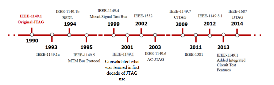
Fig.1 JTAG History Timeline1
JTAG provides a way for testing and debugging the internal connections of a device without physically accessing the individual pins. By using a set of dedicated JTAG pins on a device, engineers can perform a range of operations, such as boundary scan testing, chip programming, and debugging. Here are some of the main uses of JTAG:
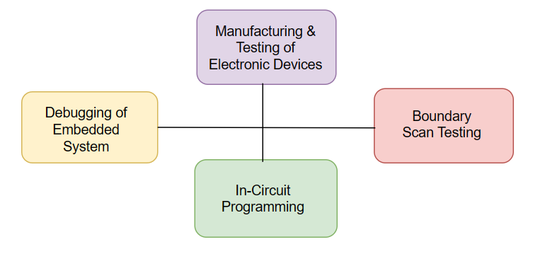
Fig.2 JTAG Usages2
Boundary Scan Technique:
Boundary-scan is an integrated method for testing interconnects on printed circuit boards (PCBs) that are implemented at the integrated circuit (IC) level. The boundary scan technique adds a set of test registers, known as boundary scan cells, to a digital circuit. These cells are connected to the input and output pins of the circuit through a serial scan chain, which can be accessed using JTAG commands. Each boundary scan cell consists of a shift register that can be loaded with test data and shifted out serially to the next cell in the scan chain. The cells can also be used to capture and observe the state of the input and output pins of the circuit.
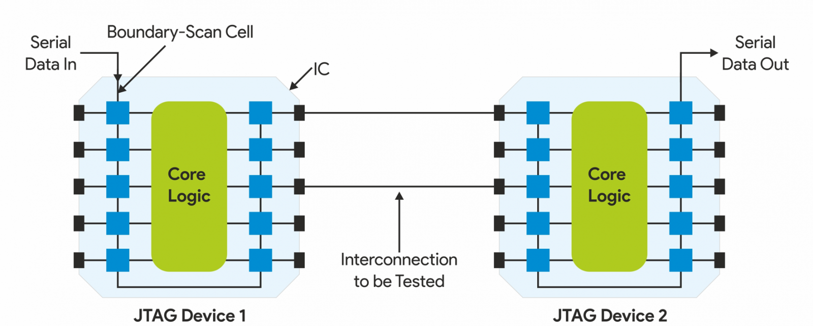
Fig.3 IEEE Std. 1149.1 Boundary-Scan Testing3
To perform a boundary scan test, the JTAG controller loads test data into the boundary scan cells and then scans the data through the scan chain. The data is applied to the input pins of the circuit, and the resulting output is captured by the boundary scan cells. The captured data can then be shifted out of the scan chain and compared to the expected output.
This BST architecture includes two main components: a shift register and a multiplexer. The shift register is used to store and shift in/out data, while the multiplexer is used to select the input or output path for the data. When the multiplexer is set to the input path, data from the external tester is scanned into the shift register through the input pin. When the multiplexer is set to the output path, data stored in the shift register is scanned out through the output pin and sent to the external tester.
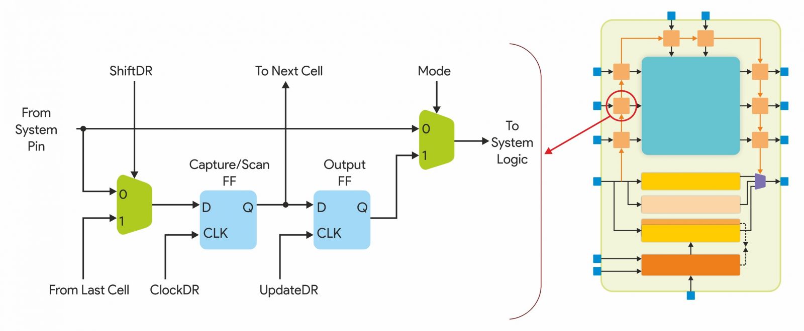
Fig.4 A Standard Boundary-Scan Cell4
JTAG Architecture
JTAG architecture comprises of four major components –
1. Test Access Port (TAP):
It is the interface used for JTAG control. The IEEE standard defines four mandatory TAP signals (TDI,TDO,TMS,TCK) and one optional TRST signal.
Table3.1 Lists the functions of each of these pins
|
PINS |
DESCRIPTION |
|
TDI (Test Data Input) |
Serial Input pin for instructions and data. Data is shifted in on the rising edge of TCK
|
|
TDO (Test Data Output) |
Serial output pin for instructions and data. Data is shifted out on the falling edge of TCK. The pin is tri-stated if data is not being shifted out of the device. |
|
TMS (Test Mode Select) |
Input pin that provides the control signal to control the transitions of TAP controller state machine. Transitions within state machine occur at the rising edge of TCK. |
|
TCK (Test Clock Input) |
The clock input to the boundary scan test circuitry. |
|
TRST (Test Reset Input ) |
Active low input asynchronously reset the TAP controller (TRST is optional according to the std IEEE1149.1) |
2. TAP Controller:
The TAP (Test Access Port) controller is a digital circuit that is used to access the individual pins of a JTAG interface. The TAP controller is responsible for controlling the data transfer between the JTAG interface and the device under test (DUT). It is typically implemented as a 16-state finite state machine (FSM) that governs the behavior of the JTAG interface.

Fig.5 JTAG TAP Controller State Transition Diagram5
3. Registers:
The instruction register is a shift register that stores the instruction being executed by the TAP controller. It is loaded with a specific instruction by shifting in the corresponding bit pattern serially through the TDI (Test Data Input) pin. Once the instruction is loaded into the instruction register, it is decoded by the TAP controller and the corresponding operation is executed.
The data register is a shift register that is used for transferring data in and out of the IC. The data register is loaded with data by shifting in the corresponding bit pattern serially through the TDI pin. Once the data is loaded into the data register, it can be shifted out serially through the TDO (Test Data Output) pin.
i. Bypass Register
The bypass register provides a mechanism for bypassing the TAP controller and allowing direct access to the IC being tested. The bypass register is useful for testing and debugging ICs that have multiple TAP controllers, or for accessing specific components of an IC that are not accessible through the TAP controller.
ii. Boundary Scan Register
The boundary scan register consists of a chain of shift registers that are connected to each of the IC's input and output pins. This allows the JTAG host to test the connections between the IC and other components on the PCB, by applying test patterns to the IC's input pins and observing the output patterns on the IC's output pins.
iii. Device ID Register (optional)
The device ID register contains a unique identifier for the IC being tested, which can be used by the JTAG host to identify and communicate with the IC. The device ID register is typically a fixed-length shift register that is loaded with a specific bit pattern during manufacturing.
4. Instruction Decoder:
The instruction decoder is a part of the Test Access Port (TAP) controller, which is used for testing and debugging integrated circuits (ICs). The instruction decoder is responsible for decoding the JTAG instructions sent by the JTAG host and executing the corresponding actions on the IC. The JTAG instructions are typically encoded as a binary value that is loaded into the instruction register. The instruction decoder reads the value of the instruction register and performs the corresponding action on the IC. The instruction decoder supports a set of standardized JTAG instructions, such as EXTEST (external test), BYPASS, SAMPLE/PRELOAD, and others.
Key Differentiation Between IJTAG & CJTAG
IJTAG (Internal Joint Test Action Group) and CJTAG (IEEE 1149.7) are both standards used for testing and debugging integrated circuits (ICs).
IJTAG is an extension of the IEEE 1149.1 boundary-scan standard, which defines a standardized method for testing the interconnects of digital circuits. IJTAG provides a standardized way of accessing the internal components of an IC for testing, configuration, and debug purposes. It allows for more efficient testing and reduces the need for external test equipment.
CJTAG is also an IEEE standard, but it is designed specifically for mixed-signal and analog devices. It is an extension of the IEEE 1149.1 and IEEE 1149.4 standards, which define test access ports (TAPs) for digital and mixed-signal circuits. CJTAG provides a standardized way of accessing the analog components of a mixed-signal IC for testing, configuration, and debugging purposes. It also supports features such as adaptive test clocking, which allows for more efficient testing of analog circuits.
In summary, while both standards are used for testing and debugging ICs, IJTAG is mainly focused on digital systems while CJTAG is focused on mixed-signal and analog devices.
Conclusion
Overall, JTAG is a versatile and powerful tool for testing, debugging, and programming electronic devices. Today, it is widely used in a variety of industries, including aerospace, automotive, telecommunications, and consumer electronics. It has become an essential tool for engineers and technicians who need to test and debug electronic circuits quickly and accurately. There are also different versions of JTAG, such as IJTAG and CJTAG, each optimized for different types of architectures and applications.
Diagram References:
D-25, 1st Floor, Lajpat Nagar -II, New Delhi 110024
+1-512-541-1878 | sales@truechip.net