
loading...
Introduction
The first generation of Synchronous DRAM (SDRAM) is SDR, which stands for Single Data Rate SDRAM. SDR can transfer only one instruction per clock cycle, which limits the speed and efficiency of data transfer. Double Data Rate SDRAM (DDR-SDRAM) is the new version of SDRAM in which data transfer is possible through both the clock edges (rising and falling edge), making it twice as fast as SDR SDRAM. Data transfer on both the clock edges is common in all generations of DDR, but each new generation brings features that make them technically very different.
Given below is a figure showing SDR vs DDR data transfer per clock.
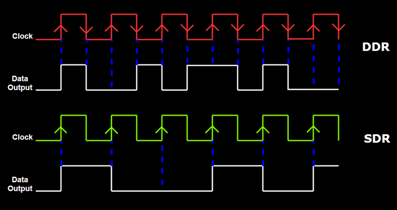
Figure.1 SDR vs DDR data transfer
As SoCs are getting more complex with the addition of more cores and functionality, low power and high performance become vital goals. DDR SDRAMs meet these memory requirements by offering high-performance, greater-density, and low-power memory solutions. DDR has improved over the years as the industry has progressed from DDR to DDR2, DDR3, DDR4, and now DDR5 SDRAM.
DDR5 is the latest and fifth generation of DDR SDRAM. This standard is able to achieve a higher data transfer rate (speed), more bandwidth, reduced operating voltage, and better efficiency. DDR5 maintains the same pin configuration as its predecessor DDR4, unlike the last transition from DDR3 to DDR4 in which the DDR3 module uses 240 pins and DDR4 uses 288 pins.
Let us see, “Why DDR5 is becoming the preferred choice?”.
Advantages of DDR5 over DDR4:
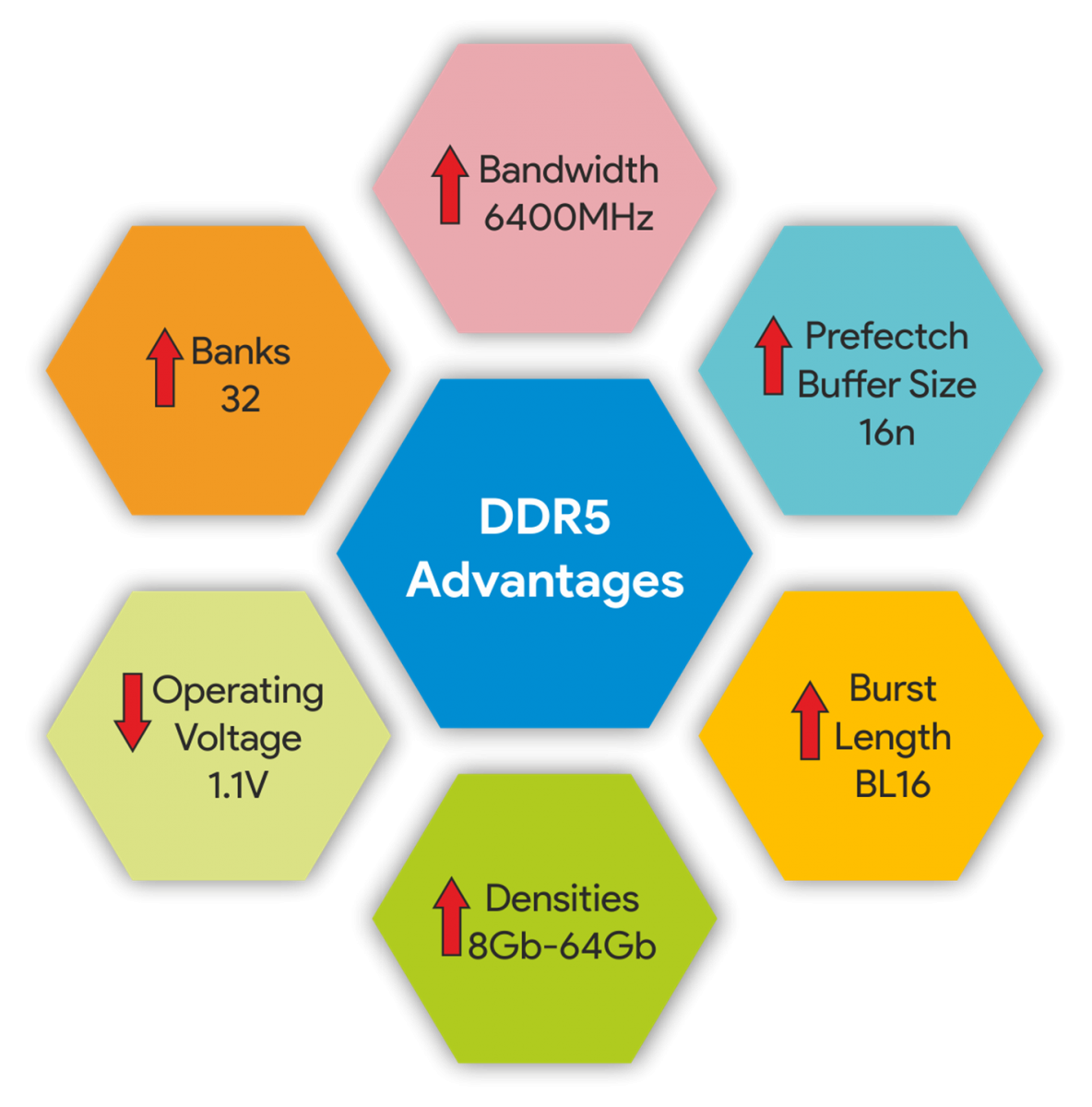
Figure2. DDR5 Advantages
Capacity:
DDR4 has a maximum memory density of 16Gb per rank, but DDR5 quadruples that number to 64Gb. DDR5 supports memory density from 8Gb to 64Gb per rank, with a wide range of data rates from 3200 MT/s to 6400 MT/s. Therefore, DDR5 sticks with much more overall capacity than DDR4.
Dual Channel DIMMs:
DDR5 supports two channels per DIMM as opposed to DDR4’s single channel. The DDR4 standard supports one 72-bit channel (that has a 64-bit data channel and an 8-bit ECC). In comparison, DDR5 Dual Channel offers two 40-bit channels with 32-bit reserved for data and 8-bit for ECC. The two independent channels improve memory access which ensures faster data transfer.
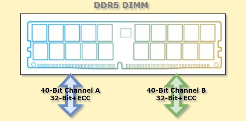
Figure 3. DDR5 Dual Memory Channel
Improved Bandwidth:
An Increase in data rate is one of the primary factors responsible for DDR5’s bandwidth increase. While DDR4 extends data rates from 1600 MT/s to 3200 MT/s, DDR5 is currently defined with data rates ranging from 3200 MT/s up to 6400 MT/s. It is safe to say that DDR5 offers up to 2x the effective bandwidth as compared to its predecessor DDR4.
The number of CPU cores has exponentially increased and it is expected to increase continuously. As the number of cores increases, the demand for memory bandwidth is also increasing. DDR4 has reached its maximum data rates and cannot continue to scale memory bandwidth with these ever-increasing core counts. DDR5 offers twice the effective bandwidth as compared to DDR4, helping relieve this bandwidth per core issue.
Furthermore, the burst length for each of those channels has been increased from 8 bytes (BL8) to 16 bytes (BL16), meaning DDR5 will be able to perform two 64-byte operations in the same amount of time it takes for DDR4 to perform a single one.
Banks:
DDR5 uses a 32-bank structure with 8 bank groups, twice as much as DDR4’s 16-bank design. DDR5 doubles the number of bank groups while keeping the number of banks per bank group the same. Increasing bank groups is important as bank access to different bank groups requires less time delay compared to bank accesses within the same bank group. Banks within the same bank groups share local I/O routing, sense amplifiers, and array blocks, which introduce longer timing constraints.
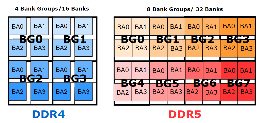
Figure 4. DDR4 & DDR5 Banks
Prefetch Buffer Size:
A Prefetch buffer is a data buffer that is used to store prefetched data for quick and easy access to multiple data words. The term Prefetch buffer size describes how many words of data are fetched every time a row is accessed. For instance, in DDR4 with a Prefetch buffer depth of 8n, eight consecutive data words are read in a single clock cycle and placed in the Prefetch buffer. Each word will then be transmitted on consecutive rising and falling edges of the clock cycle.
Over generations, the prefetch buffer size has increased from 2n to 16n. DDR4 has 8n Prefetch architecture. DDR5 has a 16n prefetch architecture, which gives it a higher speed.
Better Power Management:
Power Management Integrated Circuit (PMIC) is available in DDR5 to increase power integrity so providing power where necessary. DDR5 uses a lower voltage than DDR4, namely 1.1V instead of 1.2V. The PMIC distributes the 1.1 V VDD supply, helping with signal integrity by reducing noise, voltage drop, crosstalk, and thermal effects with better on-DIMM control of the power supply.
DDR5 Advanced Features
Larger capacity, higher speed, and better power management as mentioned above are the main improvements of DDR5 SDRAM over DDR4 but in addition to these other features have also been added & improved in DDR5 to enhance device architecture and performance. Some of the key features of DDR5 are as follows:
|
Features |
Description |
|
Power Management (PMIC) |
DDR5 regulates the power efficiently. Structure-wise, the PMIC is moved onto the DIMMs, reducing redundant power management circuitry on the motherboard for unused DIMM slots in the previous generations. The PMIC takes in the 12-V power supply from the system and performs the necessary power conversion and regulation to distribute the 1.1V VDD supply voltage to the memory modules. This makes for better power distribution compared to previous generations, improves signal integrity, and reduces noise. |
|
Internal VREF |
Internal VREFCA/CS provides a significant improvement in voltage margins for these pins, which further enables higher data rates. This can save costs by eliminating the need for an external reference voltage on the board. |
|
Burst Length |
The DDR5 default burst length (BL) has increased from 8 to 16. It supports an optional fixed BL32 mode and optional BL32 OTF (On the fly) mode for x4 devices only. |
|
Mode Registers |
DDR5 provides room to expand for new feature support and improvement as there are now 256 (8-bit) mode registers. |
|
Precharge Commands |
In addition to all bank (PREab) and per bank (PREpb) Precharge commands, DDR5 also supports the same bank Precharge (PREsb). PREsb command enables the precharging of a specific bank in each bank group, keeping the active state of all other banks unchanged. |
|
Refresh Commands |
Same Bank Refresh (REFsb) is the new addition to DDR5 refresh operations. REFsb allows refreshing a specific bank in each bank group, keeping all other banks in the bank group free to access. |
|
On-die ECC |
Strengthens on-chip RAS (Reliability, Availability, and Serviceability); reduces the burden on the controller. DDR5 ECC is implemented as single error correction (SEC), pairing 128 data bits with 8 parity bits to form a 136-bit codeword that is stored in the DRAM during a WRITE command. |
|
CRC (Cyclic Redundancy Check) |
While DDR4 supports CRC only for the WR data, DDR5 extends CRC to the RD data, allowing additional protection against errors occurring on the channel. This strengthens the system RAS by protecting read data. |
|
CA & CS Training |
CA & CS training improved the timing margin on the CA and CS pins enabling faster data rates. |
|
Equalization Techniques |
DDR5 utilizes Decision Feedback Equalization (DFE) to provide stable, reliable signal integrity on the module, required for high bandwidth. It opens up the DQ data eye inside the DRAM, directly enabling high data rates. |
|
MIR (Mirror Pin) |
DDR5 components also introduces the MIR pin. With the MIR pin connected (strapped) to VDDQ, the SDRAM internally swaps even numbered CA with the next higher odd number CA. |
|
Loopback mode |
Loopback mode enables testing of DQ and DQS signaling between the controller and the DRAM, isolating the actual memory array since read/write accesses are not needed. |
|
Bus Inversion |
With the Command/Address Inversion (CAI) pin connected (strapped) to VDDQ, DRAM internally inverts the logic level present on all the CA signals providing a significant reduction in VDDQ noise on modules. |
|
Write Pattern Command |
In the write pattern command, no data is sent on the DQ bus, no toggling of DQS is needed, and the DRAM does not turn on any internal ODT. When used effectively, the command can save power by not actually sending the data across the bus. |
|
Write Leveling Training |
DDR5 supports External WL training for cycle alignment, Internal WL training for phase alignment. Write leveling training in DDR5 compensates for the device’s unmatched DQ-DQS path, making it easier to support fast data rates with short write preambles and enabling shorter bus turnarounds. |
|
Command/Address Interface (CA [13:0]) |
DDR5 requires two cycles for some (but not all) commands, reducing the CA pin count. |
DDR5 offers higher density including a dual-channel DIMM topology for higher channel efficiency and performance. These advantages are most significant for SoCs targeting servers, cloud computing, networking, desktop, and consumer applications.
Conclusion:
The growing need for increased memory bandwidth due to scaling requirements and higher performance targets of next-generation computer systems creates an important challenge for today’s system architects. DDR5 has been developed with maximum potential capacity for a single DDR5 DIMM to 128GB, a maximum transfer speed of 6400MT/s which is doubling the rate of DDR4, along with the improved power consumption of 1.1V. DDR5 SDRAM sets the bar higher than ever before when it comes to overall system performance—pushing the limits of high-speed signaling and directly addressing the memory bandwidth challenge.
DDR5 has barely hit the shelves, and Samsung has already confirmed that it’s already working on the next generation of SDRAM. The 6th-gen DDR memory is likely to arrive in couple of years. It is expected that in DDR6 memory, data transfer rates will be doubled compared to its predecessor, and as for the number of memory channels per module, that will also be doubled for DDR6, with four 16-bit channels joined by 64 memory banks.
DDR6 References:
Samsung's next-gen DDR6 / GDDR6+ memory solutions will be 2x faster - SamMobile
Samsung DDR6 Memory Roadmap: Up To 24 Gbps Speeds For New GPUs (fossbytes.com
D-25, 1st Floor, Lajpat Nagar -II, New Delhi 110024
+1-512-541-1878 | sales@truechip.net