
loading...
DDR Verification IP stands for double data rate. It is a memory technology based on Synchronous dynamic random access memory (SDRAM). DDR SDRAM access is twice as fast as SDRAM, because DDR data transfers occurs on both edges of the clock signal as compared to SDRAM which transfers data only on the rising edge of a clock. There was another side benefits to this change as well, it meant memory could run at a lower clock rate using less energy and achieves faster speeds.
It strikes a good balance between transfer rate, cost and the power consumption.
It has high performance as it is faster and more efficient.
It supports ECC and CRC to detect and correct error. It is used to maintain the reliability of memory.
It also supports Automatic self refresh operation which depends on the operating temperature.
It is an ideal solution for numerous applications ranging from high performance computing and supercomputers, to smaller power constrained mobile devices.
As technology progressed and processors became still more powerful and demanding, DDR alone became insufficient. It was followed, in 2004 , by DDR2, with an internal clock running at half the speed of the data bus i.e. 800MT/s ; this meant it was about twice as fast as original DDR using lesser power (1.8 volts). DDR3 was next out of the gate. It debuted in 2007, with its internal clock cut in half again , its speed about twice i.e.2133MT/s that of DDR2 and power usage reduced even more over its predecessor.
The DDR4 came into existence in 2014, which has transfer rate up to 3200MT/s with voltage of 1.2 volts.
The evolution of DDR has exponential growth with applications requiring more memory, so the bandwidth increased multiple folds from DDR to DDR4 from 1GB to 16GB.
.jpg)
In 2019, the latest version of DDR i.e. DDR5 is expected to be launched.
A DIMM (dual-in-line memory module) is a double SIMM (single-in-line memory module). Like SIMM, a DIMM is a module that contains one or several random access memory chips on a small circuit board that connect it to the computer motherboard.
A SIMM typically has 32 data bit path to the computer that requires 72-pin connector. For DDR SDRAM chips, which have a 64 data bit connection to the computer, SIMMs must be installed in in-line pairs, since each supports a 32 bit path.
DIMMs eliminated the practice of pairing two SIMMs as one. A single DIMM can be used instead.
As faster dynamic random access memory was developed, DIMMs circuit boards evolved. Another evolution in DIMMs is the use of cooling fans which help vent the heat into the computer enclosure and away from the mortherboard and CPU.
DIMMs are not backward compatible to SIMMs. Application of DIMMs is not limited to PCs, it is applied to variety of electronic products that include printers, netbooks and networking hardware.
Various types of DIMMS are as follows:
Un-buffered Dual In-line memory module (UDIMM).
Small-outline Dual in-line memory module (SO-DIMM),
Micro Dual In-line memory module (Micro-DIMM).
Registered Dual In-line memory module (RDIMM).
Fully Buffered Dual In-line memory module (FB-DIMM)
and Load Reduced Dual In-line memory module (LRDIMM).
Let’s see the differentiating features between the DIMMs:
UDIMM
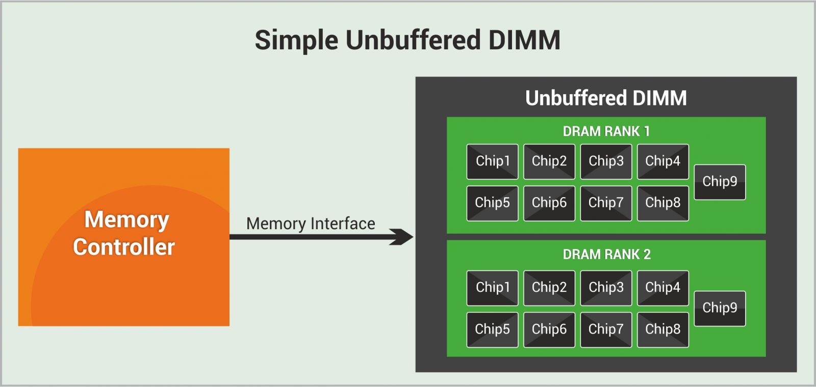
It is a type of memory chip used mostly in desktop, laptops and mobile systems. It run faster than Registered memory (RDIMM) and cost less, but they are not quite stable as RDIMMs. In UDIMMs each chip of the memory module is addressed individually and in parallel by the memory controller inside the CPU. The memory chips in use today are a type of UDIMM.
In UDIMM there is no buffering present on address and data-path between the memory controller and the DRAM. The memory controller sends all the commands directly to the DRAMs.
SODIMM and Micro DIMMs
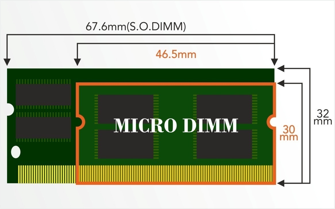
Space is at premium in notebook and small-form-factor desktop computers, making it difficult to find room for full sized memory modules. As a result, these computers use memory modules with smaller circuit boards. SO-DIMMs make it possible for a small computer to have memory capacity comparable to full-sized computers. One can identify the SO-DIMMs primarily by their size, a standard DIMM is slightly over five inches long and SO-DIMM is slightly over 2.5 inches long.
With the more functionality included in the next generation notebooks, the less space will remain for DRAM itself. Therefore need for DIMMs with smaller form factors and same densities as SO-DIMMs arose which are pre-dominantly used in notebooks. Hence, Micro-DIMM came into picture. Micro-DIMM is a memory module with nearly 50% higher bit density which requires 35% less board space than the SO-DIMM at the same memory density.
With the Micro- DIMM even new applications like ultra-mobile PCs and extremely slim and compact notebook designs are enabled.
So basically, SO-DIMM and micro – DIMM are basically Un-buffered DIMMs, with smaller area and capacity.
FB-DIMMs
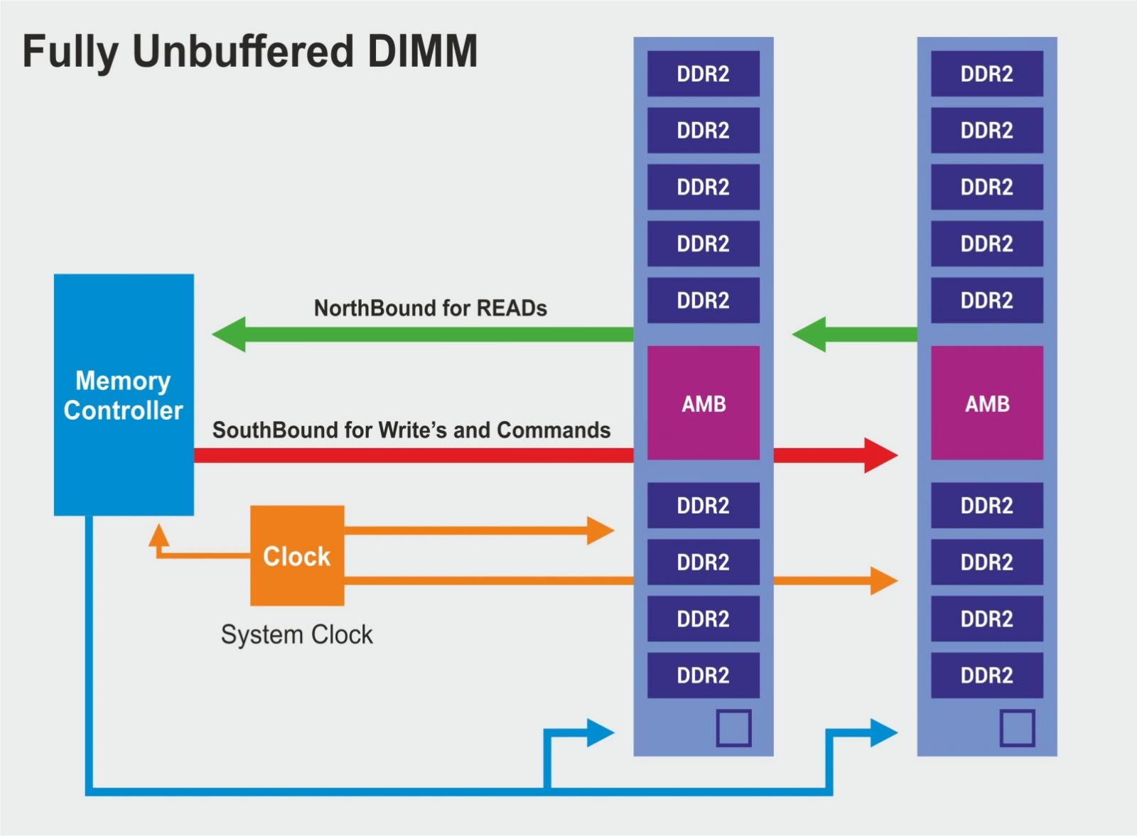
Fully Buffered DIMMs are used in servers to increase reliability and to access more memory within a system. Fully buffered DIMMs have an AMB (Advanced memory buffers). The controller sends all the memory request through AMB. Unlike other buffers this has a serial interface to the memory controller, this allows greater data width without having to increase number of pins on the memory controller Ideally, this approach reduces the physical number of signal lines at the input of DIMM and therefore, uncluttered the physical wiring with increase in number of memory module per system. . This method is only used in DDR2 modules.
RDIMMs
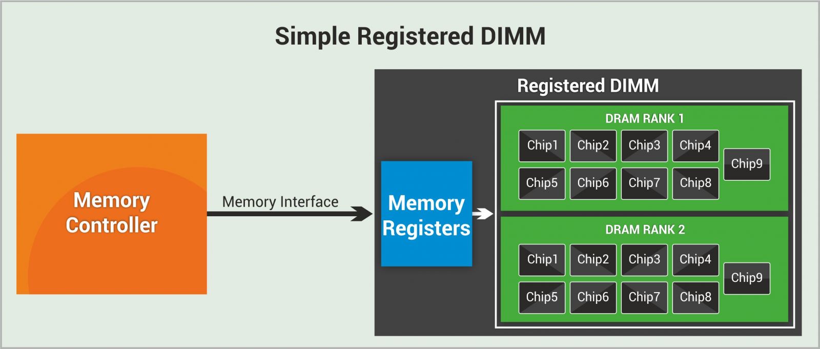
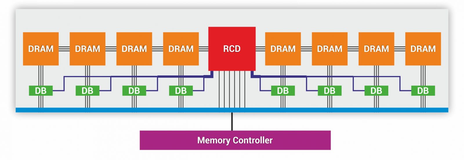
Registered DIMMs is dual in line memory module with improved reliability. The RDIMM uses a hardware register known as registered clock driver (RCD) that buffers the control signals and not the application data to the memory module. This buffering adds a clock cycle and uses more power but handles the heavier electrical loads placed on high-speed, high-density module better than tradition DIMMs. The extra clock cycle effect is over-shadowed by buffering as it reduces the load on memory controller as it points to the dedicated registers rather than accessing the DRAM directly.
This improved stability and scalability comes at a higher price, thus why RDIMMs are found mostly in servers and not desktop or laptop computers.
LRDIMMs or Load-Reduced DIMMs are a new type of industry standard memory module for servers. They are similar to Registered DIMM which are built on a memory module printed circuit boards and uses the same type of DRAM chips. That is where the similarities end, as LRDIMM function differently from Registered DIMMs.
LRDIMMs add a special memory buffer chip to the bus, affixed to each module. In RDIMM the memory bus functions in parallel mode and all DRAMs are controlled by memory controller. As more and more DRAMs are built into a RDIMM, the electrical loading of the memory module increases which results in memory speed drops. LRDIMMs can navigate outside of these restrictions through the use of memory buffers. All command and control signals are transmitted to the RCD which transfers to the memory buffer, which then handles all the reads and writes to the DRAM chips.
Basic architectural insights:
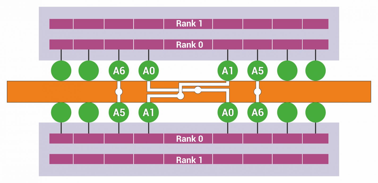
The DIMM architecture provides two unique features, namely Address Mirroring and output inversion.
Address Mirroring:
When routing connections are done it requires a lot of vias, conductor corners, long traces etc.
It does not matter how you physically route RAM array, what matters is that data written to specific location must be read from that same location, not another one.
Thus, generally, you can connect address and data pin groups of single or multiple RAM chips in any way which you see the best for routing to have shortest tracks and minimal number of vias.
The Command and Address bus pins on the DRAM are defined in a manner that allows for these short trace lengths. This allows the most flexibility with these pins. Even Rank DRAM pins are wired straight, with no mismatch between the connector pin assignment and the DRAM pin assignment. Some of the Odd Rank DRAM pins are cross wired accordingly whether they have some special function (secondary functions).
Address mirroring allows for easier routing by flipping specific pairs of address bits on Odd Ranks.
Memory Controller has to switch the address bits in an MRS command to accommodate address mirroring for correctly configuring the DRAM.
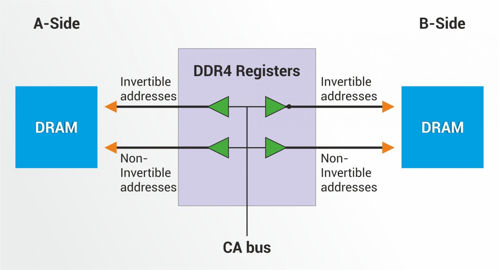
Output Inversion
In RDIMMs and LRDIMMs, output inversion is enabled inside RCD i.e. Registered Clock Driver by default. It is done to conserve power.In order to ensure that the DRAM receives the correct un-inverted MRS bits, the host-to-register-to-DRAM MRS programming is done in two steps.
Firstly, the A-side DRAMs are programmed using non-inverted addresses from the host.
Then, B-side DRAMs are programmed using inverted addresses for the invertible address signals and non-inverted addresses for the non-invertible address signals from the host.
The table below shows different configuring methods for RDIMM and LRDIMM.
Configuring , Register Clock Driver(RCD) using Register Control Word (RCW).
There are two methods to configure RCD.
First method: The memory controller configures internal registers of RCD known as Register Control Word by sending Mode Register 7 command. For reads, an RCW command is sent by the controller to the RCD to move the specific register configuration into a special multi-purpose register in the DRAM. Then the data of MPR is read out onto Controller.
Second Method is through Inter Integrated Circuit also known as I2C.There is a SPD or Serial Presence Detect module on the DIMMs. The entire configuration is set into the SPD module. Through I2C the configuration is sent from SPD to RCD. The memory controller sends all the command to RCD, which sends to the DRAM.
The memory Controller configures Data buffer through RCD.
RCD configures the internal registers of Data Buffer using Buffer Control Word.
Mode Register 7 is used for configuring DB.
When A[12] bit of Mode Register 7 is 1 , it’s used for configuring Data Buffer , otherwise for configuring RCD.
The microcontroller can read out the DB buffers configuration by sending buffer control word command through RCD , to read out from the multi-purpose register of data buffer.
I2C configures Data Buffer through RCD.
Configuring DRAM using MRS:
Memory Controller sends all the configuration of DRAM to RCD through MRS commands i.e MRS0 to MRS6.
RCD send all the configurations to the DRAM.
The configuration set in DRAM can be read out through Multi-Purpose Register (MPR) Read command.
DRAM and RCD both support even parity.
Future RoadMap:
Non-volatile Dual inline memory modules are a brand new and very different storage technology. NVDIMMs replaces the traditional memory sticks in a server and allows the data to remain in place when the power is removed from the system. This is achieved by adding flash to the DRAM on the DIMM. When power goes away, either deliberately or by a failure, the data from the DRAM is copied into a NAND flash memory. This allows the data to be instantly available, without reloading from the device, when the power is restored.
There are two distinct NVDIMM models available, both promises the huge performance benefits and are poised to impact everything from data centers to Smartphone.
One type- NVDIMM-N uses a lot of DRAM, about 16GB per DIMM, and matches with an equal amount of flash. This type of DIMM is fast as data transfers at DRAM speeds back and forth. It is best suited for use where the speed of access to persistent data is very important but it is limited to around a terabyte if total memory today.
Another type of NVDIMM, NVDIMM-F uses a small amount of DRAM as a buffer to a very large flash. This DRAM bus is used to read and write into the large flash memory, as much as several terabytes per DIMM pair.
NVDIMM-F is slower than NVDIMM-N. Application of Non-volatile DIMM cards is , it may be used to extend system memory or supply high performance storage. By end of 2018 another type of NVDIMM-P is to be launched.
D-25, 1st Floor, Lajpat Nagar -II, New Delhi 110024
+1-512-541-1878 | sales@truechip.net